Reliable Industrial PCB Solutions for Unmatched Performance
Precision Engineering for Next-Generation Industrial Systems
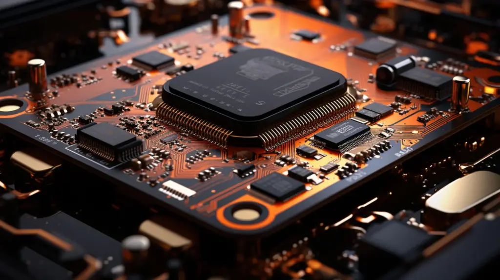
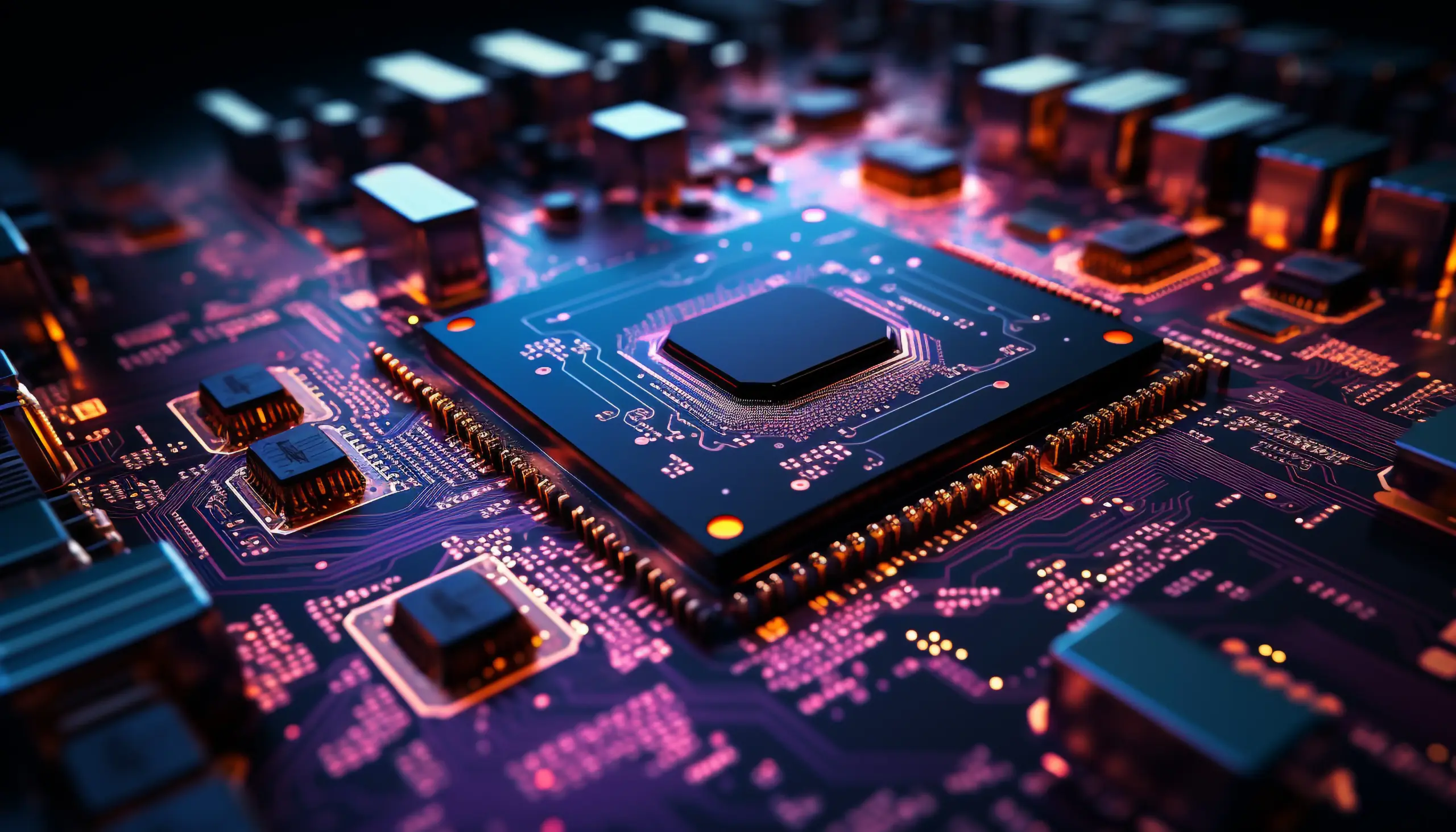
Printed Circuit Boards (PCBs) are present in every modern electronic device. Be it a smartphone, an industrial control panel, or robotics, PCBs connect the link between innovation and functionality. PCB industrial engineering in India takes
this concept a notch higher, focusing on robust designs that meet the stringent demands of heavy-duty applications. This field combines precision and creativity to ensure your manufacturing processes deliver consistent performance with every unit produced.

Custom PCB Solutions for Industrial Applications
Ever since its establishment in 2021, Elventive Pvt. Ltd. has quickly become a trusted name in industrial PCB engineering in India. We provide precise and dependable solutions that power industries by fusing modern technology with a thorough understanding of manufacturing challenges. Every PCB we design reflects a commitment to quality, durability, and performance. Our engineers work closely with clients to customize designs that not only fit but enhance their operations. The result is bringing boards in the market that can handle the heat—literally and figuratively—while meeting rigorous industry standards. From prototyping to full-scale production, our processes ensure that every PCB matches your exact specifications.
The Value of Custom Solutions in Industrial PCB Engineering
Industrial manufacturing often involves unique operational needs throughout its production line that require personalized PCB solutions. Off-the-shelf designs may not align with the specific demands of a given application, especially in sectors like automation, heavy machinery, or high-tech production lines. Custom PCBs are engineered to address these challenges, ensuring compatibility with the intended environment and operation.
Precision in customization allows industrial PCBs to:
1) Handle extreme temperatures and vibrations.
2) Optimize performance in compact or high-power devices.
3) Align with specific design constraints or workflow requirements.
4) Minimize errors and ensure seamless integration within larger systems.

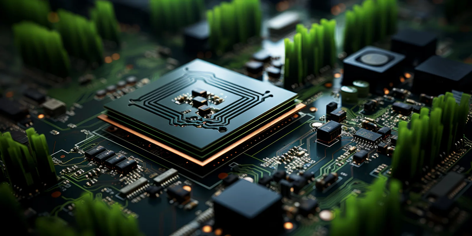
Types of Industrial PCBs Procured By Elventive
Industrial PCB designs vary significantly based on their application and operational demands. Each type serves a unique purpose, contributing to the overall functionality of industrial systems.
1. Single-layer PCBs
These are the simplest type of PCBs, featuring a single conductive layer. Though basic in design, they are highly effective for straightforward applications like LED lighting systems or entry-level control mechanisms. Their simplicity makes them cost-effective and reliable for less complex operations.
2. Multi-layer PCBs
Multi-layer PCBs stack several conductive layers, enabling compact designs with enhanced performance. They are used in advanced industrial devices such as communication modules, power supply systems, and data processors.
3. Rigid PCBs
Known for their structural stability, rigid PCBs are ideal for heavy-duty applications. They are commonly used in systems that prioritize robustness, such as industrial automation equipment, where mechanical stress and constant operation are routine.
4. Flexible PCBs
Flexible PCBs are designed to bend and adapt without breaking, making them invaluable in applications that require dynamic motion. These are often found in robotics, wearables, and movable machinery where flexibility is crucial to functionality.
5. Metal-core PCBs
Metal-core PCBs incorporate a metal base layer, typically aluminum or copper, to manage heat dissipation effectively. These are essential in high-power applications like industrial LED modules and motor controllers, where temperature regulation is critical to maintaining performance.
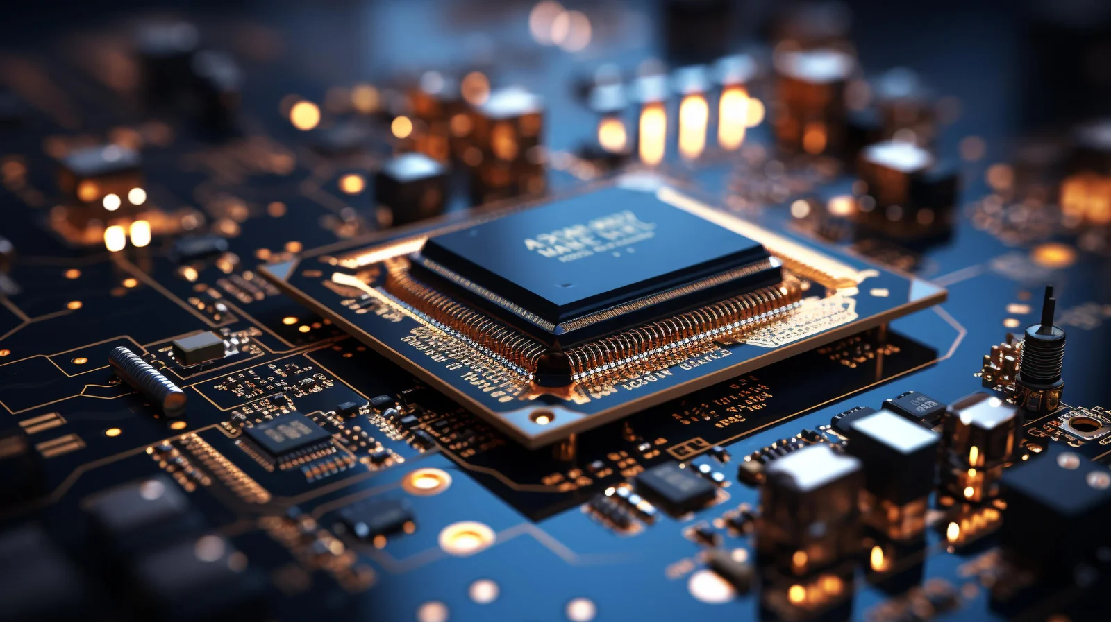
Core Principles of Industrial PCB Design
Creating a reliable PCB for industrial applications requires careful consideration of various design elements. Each principle contributes to the board’s ability to function optimally under rigorous conditions.
Every component has a space to thrive. Our PCB footprint creation process ensures that every part fits perfectly, optimizing the overall design. Every footprint, whether it’s a tiny sensor or a sophisticated
microprocessor, is designed for smooth integration, improving both usefulness and manufacturing viability.
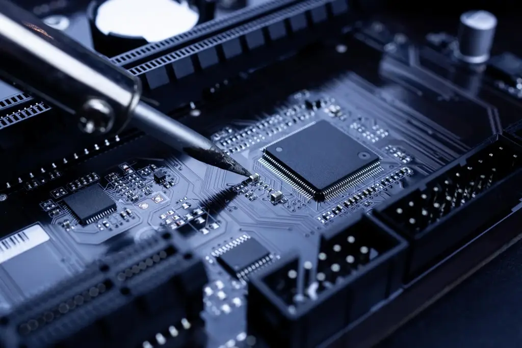
Development Stages of Industrial PCB Engineering
The development of industrial PCBs follows a systematic process designed to meet the exacting demands of modern manufacturing.
-
Needs Assessment Step 1
Understanding the operational requirements is the first step. This involves evaluating the environmental conditions, performance expectations, and integration challenges the PCB will face.
-
Design and Simulation Step 2
Advanced CAD tools are used to create detailed PCB layouts, simulating their performance under real-world conditions. This stage identifies potential issues and optimizes the design before physical production begins.
-
Prototyping Step 3
Prototypes are fabricated to test the design’s functionality and reliability. By evaluating these early models, adjustments can be made to ensure the final product meets all specifications.
-
Manufacturing Step 4
The final design is manufactured using precision techniques that ensure consistency across all units. High-quality materials and processes guarantee the durability and performance of the finished boards.
-
Quality Assurance Step 5
Before deployment, every PCB undergoes rigorous testing to verify its durability, accuracy, and compliance with industry standards. This stage ensures that only flawless boards enter the market.
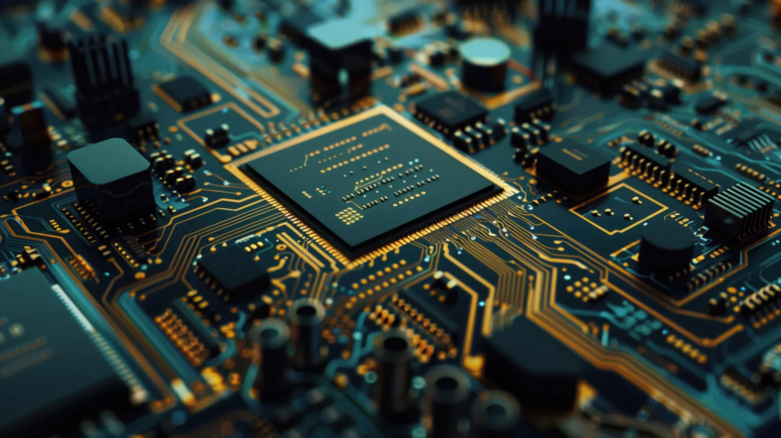
Technological Integration in PCB Engineering
Modern industrial PCB engineering in India leverages the following set of technology to achieve precision and efficiency.
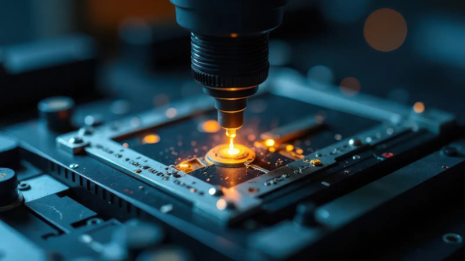
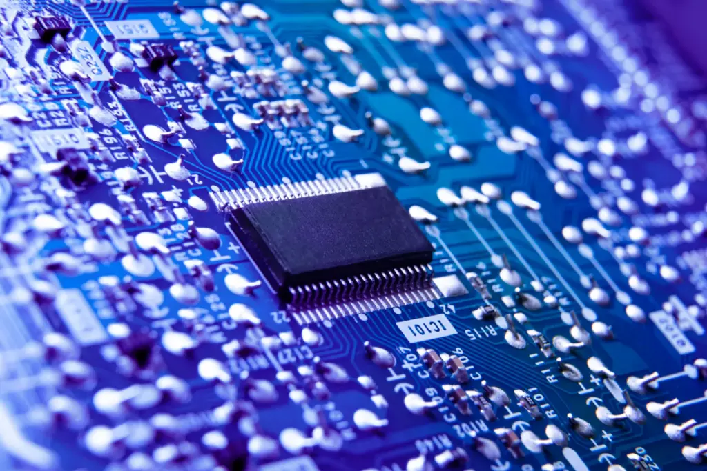
Reflow Soldering
Reflow soldering ensures strong, reliable connections by melting solder to secure components to the board. This process is controlled with precision to prevent defects and ensure consistent results.
AOI systems are used to detect manufacturing defects during production. By identifying errors early, these systems save time and reduce costs associated with rework or rejected batches.

Make An Impact With Industrial PCB Engineering
Modern manufacturing capabilities are advanced in a substantial way solely by the help of PCB industrial engineering in India. These boards promote efficient workflows across industries with the use of designs that put a major priority on accuracy, resilience, and functionality. Let’s contribute to a future where technology and productivity go hand in hand!
FAQ
1. What does PCB stand for in the context of industrial engineering?
PCB stands for printed circuit board, a foundational component in industrial engineering that supports electrical connections and mechanical functions in electronic devices. An industrial PCB is major needed in industries like automotive, telecommunications, and healthcare. This modern PCB design and assembly focuses on optimizing signal integrity and thermal management. With advanced manufacturing techniques, industrial PCB engineers ensure robust and efficient circuit designs. The growing demand for electronics in India highlights the importance of industrial PCB solutions to enhance performance and reliability across sectors.
2. What is industrial PCB design?
An Industrial PCB design refers to circuit boards that can handle the burden of industrial applications. It includes designing layouts, ensuring signal integrity, and accommodating harsh environments. Industrial PCB engineering involves advanced techniques like multilayer PCB design, flexible PCBs, and thermal management solutions. This ensures reliability and durability in industries like aerospace and defense. Industrial PCB design represents optimization for high performance and cost efficiency, aligning with the expanding demand for industrial-grade electronics in India’s rapidly growing industrial sector.
3. What software tools are commonly used for PCB design in India?
Popular software tools for industrial PCB design in India include Altium Designer, Eagle, KiCAD, and OrCAD. These tools enable industrial PCB engineers to create precise layouts, optimize signal pathways, and perform simulations for design validation. They support high-complexity projects, including multilayer and rigid- flex PCBs. As industrial PCB engineering advances in India, software with features like thermal analysis and 3D visualization is increasingly essential. These tools create a supportive window for meeting the standards of industrial PCB engineering.
4. What is the importance of quality control in the PCB industry?
Quality control is critical in the PCB industry to ensure functionality, safety, and compliance with standards. Industrial PCB engineering in India relies on strict quality checks, including electrical testing, thermal stress tests, and automated optical inspections. Quality assurance minimizes defects, enhances reliability, and boosts the lifespan of PCBs in industrial applications. Adhering to ISO and IPC standards, industrial PCB design in India ensures global competitiveness. Effective quality control supports India’s growing electronics manufacturing sector by meeting high customer expectations in diverse industries.
5. What trends are shaping the future of PCB engineering in India?
The important trends that are currently shaping industrial PCB engineering in India include miniaturization, eco-friendly materials, and advancements in AI-driven design tools. The rise of smart manufacturing is integrating IoT-enabled PCBs for better connectivity and automation. Industrial PCB design now speaks for flexible and rigid-flex PCBs to meet complex industrial needs. With India’s push for self-reliance in electronics manufacturing, indigenous innovations in industrial PCB engineering are accelerating. The adoption of 5G, EVs, and renewable energy technologies is further driving the evolution of PCB industrial engineering in India.